
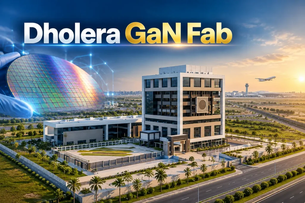
India’s chip story just added a bright new chapter. And this time, it glows.
The Union Cabinet has approved Crystal Matrix’s project under the Compound Semiconductor Scheme of the India Semiconductor Mission (ISM). The result is the Dholera GaN fab, India’s first compound semiconductor GaN fab and ATMP facility, built for the Mini/Micro-LED ecosystem.
It’s a big move for Dholera. And an even bigger one for India’s display-tech ambitions.
Not Silicon, But Something Smarter

Most chip conversations in India revolve around silicon. This one doesn’t.
The Dholera facility will work with Gallium Nitride (GaN), a compound semiconductor. That makes it the country’s first dedicated GaN fab paired with ATMP (Assembly, Testing, Marking and Packaging) capability.
In simple words, one campus handles both the making and the finishing. Wafers go in. Ready display panels come out.
That kind of integration cuts import dependence and keeps value creation within India.
The Project in Numbers
Here’s a quick snapshot of what has been approved:
| Parameter | Details |
| Company | Crystal Matrix |
| Location | Dholera SIR, Gujarat |
| Investment | ₹3,068 crore |
| Land Allotted | 40 acres |
| Scheme | Compound Semiconductor Scheme, ISM |
| GaN Wafer Capacity | 24,000 sets (each) of RGB GaN wafers per year |
| Display Panel Capacity | 72,000 sq. m of Mini/Micro-LED panels per year |
| Direct Jobs | 1,600+ |
Numbers like these signal intent. This isn’t a pilot line. It’s a production-scale plant.
Two Products, One Vision
The plant has a sharp two-part product focus.
GaN Epitaxy Wafers Epitaxy means growing ultra-thin crystal layers on a base wafer. GaN epitaxy wafers form the light-emitting heart of LED chips. The facility will produce RGB (red, green, blue) wafer sets, the building blocks of full-colour displays.
Mini/Micro-LED Display Panels These are next-generation screens that use thousands, even millions, of tiny LEDs as individual light sources.
Compared with conventional displays, they offer:
- Higher brightness
- Deeper contrast
- Better energy efficiency
- Longer lifespan
Expect them in premium TVs, video walls, car dashboards, wearables and AR/VR headsets.
Why GaN Is a Game-Changer
GaN isn’t just another material. It’s a performance upgrade.
It handles higher voltages, tolerates more heat and switches faster than silicon. That’s why it already powers fast chargers, 5G equipment and electric-vehicle electronics.
In displays, GaN is what makes bright blue and green micro-LEDs possible. No GaN, no vivid micro-LED screen.
By building GaN capability at home, India secures a material that sits at the crossroads of displays, power electronics and telecom. Today it’s panels. Tomorrow, the same know-how could feed other high-growth sectors.
Dholera’s Growing Chip Credentials
Dholera Special Investment Region (SIR) in Gujarat is steadily becoming India’s chip capital.
It already hosts Tata Electronics’ semiconductor fab project, India’s first commercial fab. Now, Crystal Matrix adds compound semiconductors to the mix.
Why do companies keep picking Dholera? A few reasons stand out:
- Planned infrastructure: Large land parcels with power and water designed for heavy industry.
- Policy backing: Support from both central and Gujarat state semiconductor policies.
- Connectivity: Close to Ahmedabad, with expressway and airport links taking shape.
- Cluster effect: Every new fab pulls in suppliers, gas providers and service firms.
With each approval, the ecosystem grows denser. And density is exactly what semiconductors need to thrive.
Jobs, Skills and Local Growth
The project is expected to create more than 1,600 direct jobs.
These are high-value roles: process engineers, cleanroom technicians, quality specialists and equipment experts. It’s precisely the skilled workforce India needs in this sector.
Indirect employment will likely be far higher. Logistics, housing, construction, maintenance and local services all grow around a fab.
For Gujarat’s students and technical institutes, this is a real opening. Industry-linked training could turn Dholera into a talent pipeline for the whole chip industry.
A Step Toward Self-Reliance
India imports almost all of its display panels and a large share of its semiconductors. That’s a strategic weak spot.
The India Semiconductor Mission is tackling it step by step. Silicon fabs and packaging units came first. Now compound semiconductors are joining the list.
Crystal Matrix’s Dholera facility fills a gap that was nearly empty. It supports Make in India, strengthens supply chains and moves the country closer to a resilient electronics base.
It also puts India early into micro-LED, a technology still maturing worldwide. Getting in now means growing with the market instead of chasing it later.
The Road Ahead
Dholera is no longer a city on paper. It’s becoming a working semiconductor corridor.
With GaN wafers and Mini/Micro-LED panels on its roadmap, the region is stepping into the future of displays and power electronics. For India, it’s one more confident step toward building chips, and screens, on its own terms.
FAQs
India’s first compound semiconductor GaN fab and ATMP facility, set up by Crystal Matrix in Dholera SIR.
₹3,068 crore.
GaN epitaxy wafers and Mini/Micro-LED display panels.
24,000 sets (each) of RGB GaN wafers and 72,000 sq. m of display panels.
Over 1,600 direct jobs.