For four years, “India’s first made-in-India chip” was a sentence spoken at podiums. Ashwini Vaishnaw said it at Davos in January 2024, targeting December of that year. He said it again in Bengaluru in February 2025, this time promising September or October. He said it once more in Hyderabad that July.
Deadlines moved. That is what happens with semiconductor fabs everywhere in the world, not just in Gujarat.
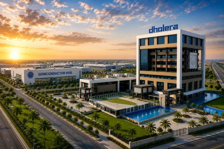
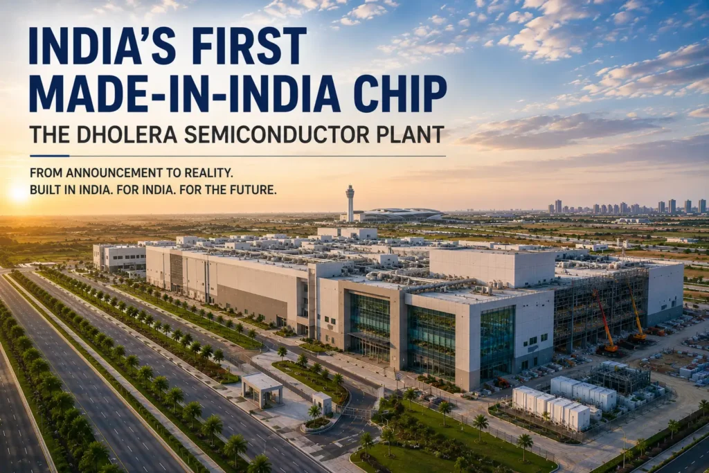
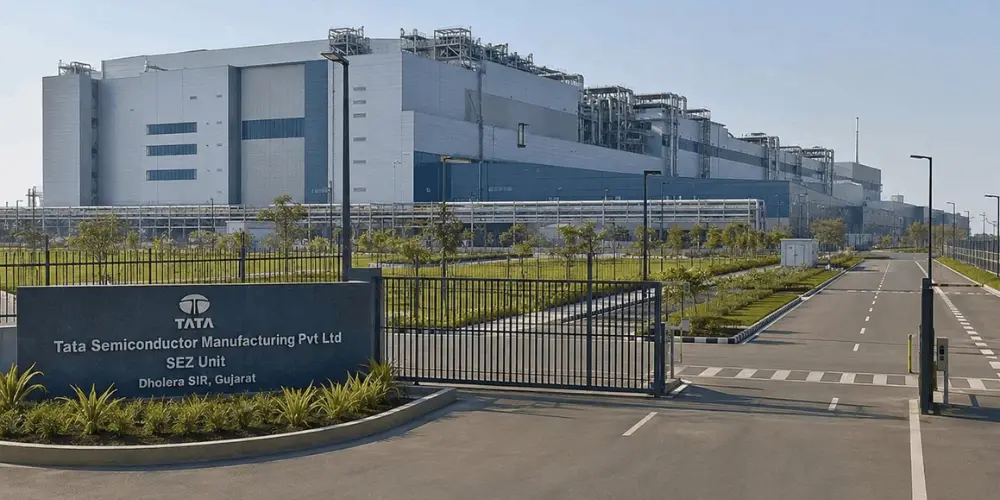
What changed in 2026 is that the argument stopped being about announcements and started being about concrete, cleanrooms and calibration. The Dholera semiconductor plant is no longer a rendering. It is a building with a schedule, a supplier list, and a set of very hard engineering problems that are now being solved one at a time.
Here is where things genuinely stand.
Tata Electronics, in partnership with Taiwan’s Powerchip Dholera Semiconductor Manufacturing Corporation (PSMC), is building a 300mm (12-inch) wafer fabrication plant in the Dholera Special Investment Region. The investment is roughly ₹91,000 crore — about $11 billion — making it the single largest project under the India Semiconductor Mission. Designed capacity is 50,000 wafers per month. It sits under the Semicon India programme, which Prime Minister Narendra Modi approved in December 2021 with a ₹76,000 crore outlay.
That is the headline. The detail underneath it is more interesting.
Construction: Past the Halfway Mark
By April 2026, construction had crossed 50% completion. Foundations are finished. The site has moved into the two phases that actually determine whether a fab works at all: cleanroom installation and equipment calibration.
This distinction matters more than most coverage suggests. In a chip fab, the concrete is the cheap part. The expensive part is the air. A cleanroom must hold particle counts, temperature, humidity and vibration inside tolerances that would be considered absurd anywhere else in industry. One speck of dust in the wrong place kills a die.
The Dholera site was also formally declared a Special Economic Zone in April 2026, unlocking the customs and tax treatment that imported fab equipment needs.
The ASML Signature
In May 2026, Tata Electronics signed a Memorandum of Understanding with ASML — the Dutch company that holds an effective monopoly on advanced lithography. Under the agreement, ASML will supply its lithography tools and support the ramp-up of the Dholera fab, alongside cooperation on local talent development, supply chain resilience and R&D infrastructure.
The timing was not incidental. Lithography scanners carry lead times of 18 to 24 months. Signing in mid-2026 is what makes a late-2026 or 2027 tool installation physically possible. It is the least glamorous and most load-bearing announcement the project has produced.
Timelines: What to Actually Expect
Trial production is targeted for December 2026. Commercial output is expected to scale progressively through 2027 and 2028 toward the full 50,000-wafer-per-month figure.
A note of realism is warranted. Reporting through 2026 has raised questions about which process node the fab will open at. The original public commitment was 28nm; some reports suggest the debut may come at a more mature node, with full commercial production pushed toward 2028. Tata’s own foundry materials describe a range of 28nm to 110nm for analog and logic ICs.
For anyone tracking this seriously, treat December 2026 as a trial-production milestone, not a retail-chip launch date. And treat node claims as provisional until wafers actually run.
What Dholera Will Make
Not smartphone processors. That is the most common misconception.
The Dholera fab targets mature and specialty nodes, which cover roughly 60% of global chip volume by unit — power management ICs, display drivers, microcontrollers, automotive electronics, and high-performance compute parts. These are the chips that go into EVs, telecom equipment, defence systems, consumer appliances and industrial controls. They are unglamorous, enormously profitable, and precisely where a new entrant can compete.
The Infrastructure That Made It Possible
A fab needs three things in absurd quantities: power, ultrapure water, and stable logistics. Dholera SIR was built to supply them before the fab arrived.
- Ahmedabad–Dholera Expressway — the ₹5,100 crore corridor opened in March 2026, cutting travel time to roughly 45–50 minutes.
- Dholera International Airport — the 3,200-metre Code 4E runway is complete, with the project in licensing, calibration and operational trial stages.
- Semi-high-speed rail — a ₹20,667 crore Ahmedabad–Dholera corridor received Cabinet approval in May 2026.
- Power and utilities — a 765 kV substation, a 250 MW operational solar park, and smart roads with underground water, drainage, power and fibre.
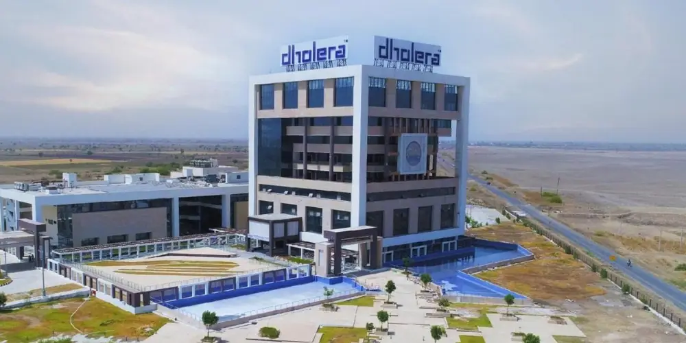
- ABCD Building — the administrative hub, fully functional, running city water, traffic and power off a centralised ICT dashboard.
Corporate MoUs for the Dholera semiconductor ecosystem can be renegotiated, but sanctioned government infrastructure generally gets built. That asymmetry is one of the strongest arguments in Dholera’s favour.
The Wider Picture
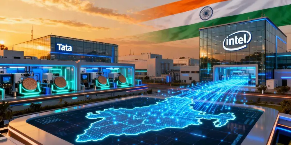
Dholera Semiconductor growth is part of Gujarat’s wider semiconductor ecosystem. Micron’s assembly and testing plant in Sanand was inaugurated in February 2026, followed by Kaynes Semicon’s OSAT facility in March. By mid-2026, three of India’s twelve approved commercial semiconductor facilities were operational.
The gap the mission has now identified is upstream: over 90% of the equipment and 85–90% of the specialty chemicals these fabs consume are still imported. Semicon 2.0, with a $13.4 billion outlay, is aimed squarely at that. Semicon India 2026, scheduled for 17–19 September, is the next checkpoint for announcements.
The Honest Takeaway
Dholera has moved from a promise to a project with a critical path. That is real progress, and it deserves to be described accurately rather than breathlessly. Fabs are among the hardest structures humans build. Slipped dates are the norm globally, not a sign of Indian exceptionalism.
For the Dholera semiconductor project, watch three things over the next twelve months: cleanroom certification, the arrival of ASML tooling on-site, and the first confirmed wafer run. Those are the real signals. Everything else is a press conference.
Frequently Asked Questions
In the Dholera Special Investment Region, roughly 100 km from Ahmedabad in Gujarat’s Bhavnagar district.
Tata Electronics, in partnership with Taiwan’s Powerchip Semiconductor Manufacturing Corporation (PSMC), under the India Semiconductor Mission.
Trial production is targeted for December 2026, with commercial output scaling through 2027 and 2028.
Approximately ₹91,000 crore (about $11 billion), the largest single project under Semicon India.
Power management ICs, display drivers, microcontrollers, automotive chips and compute parts on mature and specialty nodes.