
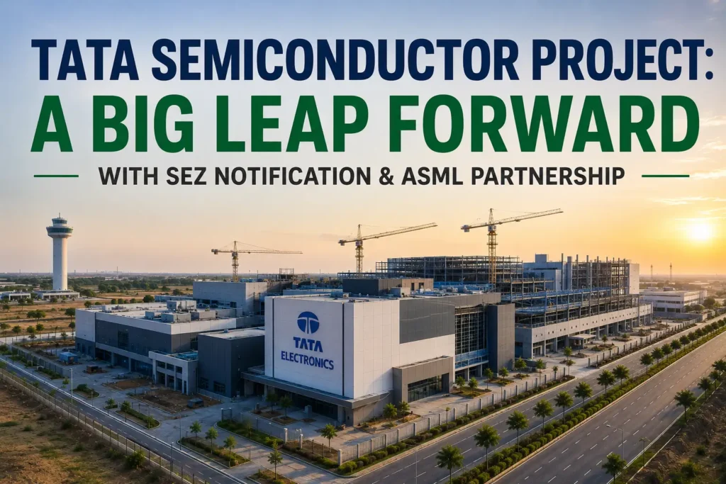
India’s dream of building its own chips at home is turning into concrete, steel, cleanrooms, and now, official paperwork. The Tata Semiconductor Project in Dholera, Gujarat, has just crossed two major milestones that push it firmly from “under construction” to “coming to life.” The Government of India has formally notified a Special Economic Zone (SEZ) for the ₹91,000 crore chip fabrication plant, and Tata Electronics has signed a strategic partnership with ASML, the world’s leading lithography equipment maker. Together, these developments mark one of the most significant weeks yet for India’s semiconductor ambitions.
1. Government Officially Notifies the Dholera SEZ
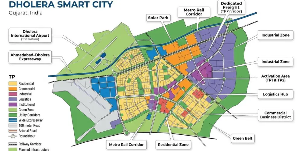
The Ministry of Commerce and Industry has formally notified the SEZ for Tata Semiconductor Manufacturing Private Limited at Dholera, spread across 66.166 hectares of land within the Dholera Special Investment Region. This isn’t just a bureaucratic formality — SEZ status brings tax benefits, streamlined customs procedures, and a dedicated approval mechanism designed specifically for large, capital-intensive manufacturing projects like chip fabs. The zone will support electronic hardware, software, and IT-enabled services, backed by enabling infrastructure to keep operations and logistics running smoothly.
2. The Policy Change That Made It Possible
The notification became possible only after the government amended SEZ Rules, 2006 in June 2025, reducing the minimum land requirement for semiconductor and electronics SEZs from 50 hectares to just 10 hectares. This single change removed a major regulatory bottleneck that had made it difficult for chip manufacturing projects, which often work with irregular or phased land parcels, to qualify for SEZ benefits in the first place. Additional flexibility in encumbrance norms and Net Foreign Exchange calculations further eased the path for large-scale fabs.
3. Scale of the Project: Investment and Jobs
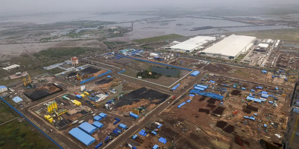
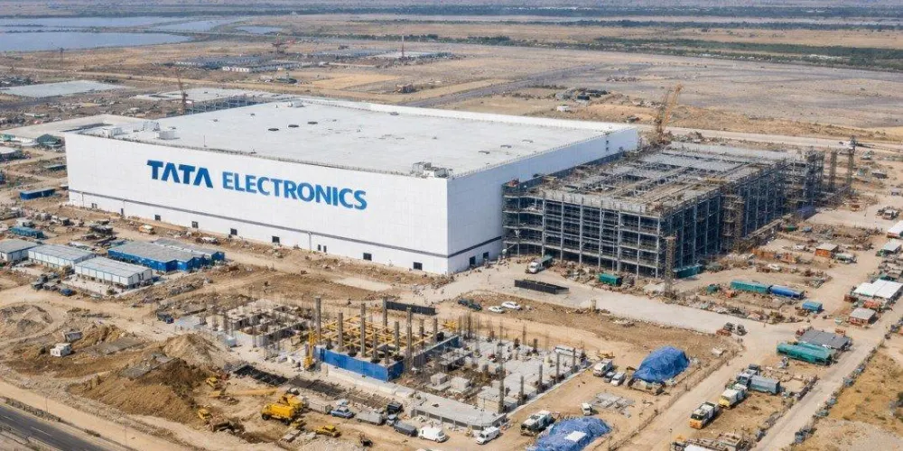
The numbers behind the project remain staggering. The Tata Semiconductor Project carries an estimated investment of ₹91,000 crore and is expected to generate close to 21,000 direct employment opportunities once fully operational. This positions Dholera as a genuine semiconductor manufacturing hub rather than just another industrial zone on a map. It is being described as India’s first commercial chip fabrication plant — a facility where raw silicon wafers are actually turned into finished semiconductor chips, unlike assembly or packaging units that handle chips made elsewhere.
4. From Cabinet Approval to Ground Reality
The fab was originally approved by the Union Cabinet in February 2024, and it is being developed in partnership with Taiwan’s Powerchip Semiconductor Manufacturing Corporation (PSMC), giving Tata Electronics access to process technology nodes ranging from 28nm to 110nm. Commercial operations are expected to begin around 2027, with a planned capacity of 50,000 wafer starts per month — enough to produce roughly 3 billion chips annually once the plant hits full stride.
5. ASML Joins Hands with Tata Electronics
If the SEZ notification is about regulatory readiness, the new ASML partnership is about technological muscle. Tata Electronics and ASML, the Dutch company that makes the highly specialized lithography machines used to print circuit patterns onto silicon wafers, have signed a Memorandum of Understanding to support the Dholera fab. Lithography is arguably the single most critical — and most difficult — step in chip manufacturing, and ASML is essentially the only company in the world capable of building the most advanced lithography systems used by leading chipmakers globally. Bringing ASML into the Dholera project signals that Tata Electronics is serious about building a fab that can compete on global quality standards, not just serve domestic demand.
6. What the Partnership Actually Covers
Under the partnership, ASML will supply its full suite of lithography tools and solutions to help establish and ramp up the 300mm (12-inch) semiconductor fab. But the collaboration goes beyond just equipment. It also includes training local talent in lithography-intensive skills, building supply chain resilience, and jointly developing R&D infrastructure that will support the fab’s long-term success. Randhir Thakur, CEO & MD of Tata Electronics, called it a “foundational partnership” that will help ensure the timely ramp-up of the fab while building a strong semiconductor ecosystem within India. Once operational, the facility is expected to manufacture chips for automotive electronics, mobile devices, artificial intelligence systems, and high-performance computing.
7. Why This Matters for India’s Semiconductor Mission
Taken together, the SEZ notification and the ASML partnership represent the kind of progress that moves a project from announcement to reality. Regulatory clearance solves the “can we legally and efficiently operate here” problem, while the ASML deal solves the “can we actually manufacture world-class chips here” problem. Both pieces need to fall into place for India’s first fab to succeed. The Tata Semiconductor Project is now widely seen as the flagship of India’s broader semiconductor mission, which also includes Tata’s separate assembly and testing unit in Assam and other approved projects across the country. If Dholera delivers on its 2027 timeline, it won’t just be a win for Tata Electronics — it will mark India’s arrival as a genuine player in global chip manufacturing, a sector long dominated by Taiwan, South Korea, and the United States. For now, all eyes remain on Dholera, where cranes, cleanrooms, and now cutting-edge lithography technology are steadily building toward that goal.
FAQs
India’s first commercial chip fab, being built in Dholera, Gujarat, at an investment of ₹91,000 crore.
It gives the project official SEZ status over 66.166 hectares, with tax and customs benefits
Around 21,000 direct employment opportunities.
ASML will supply lithography tools and support talent training and R&D for the Dholera fab.
Commercial production is expected to begin around 2027.