
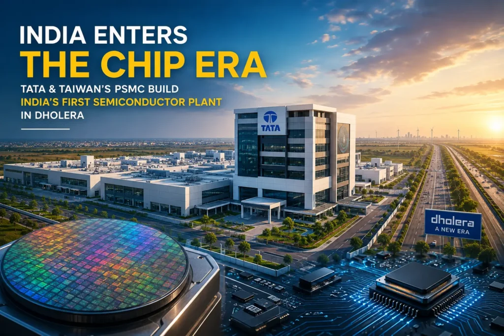
For years, every phone, car and laptop sold in India ran on chips made somewhere else. That is now changing. The Tata Semiconductor Dholera project — a partnership between Tata Electronics and Taiwan’s Powerchip Semiconductor Manufacturing Corporation (PSMC) — is building India’s first commercial semiconductor fabrication plant in Dholera, Gujarat. It is one of the biggest industrial bets India has ever made, and it is quietly reshaping a stretch of land that was mostly empty a decade ago.
What Exactly Is the Tata Semiconductor Dholera Project?
The project is a greenfield 300mm (12-inch) wafer fab being built with an investment of up to ₹91,000 crore (around US$11 billion). Tata Electronics is the owner and operator. PSMC of Taiwan is the technology partner, transferring process know-how, training people and connecting India to a ready-made supplier network.
Put simply: Tata brings the capital, the land and the workforce. PSMC brings decades of hard-won manufacturing experience. Together they are attempting something no Indian company has pulled off before — running a full-scale chip fab on Indian soil.
Why Dholera SIR Was Chosen
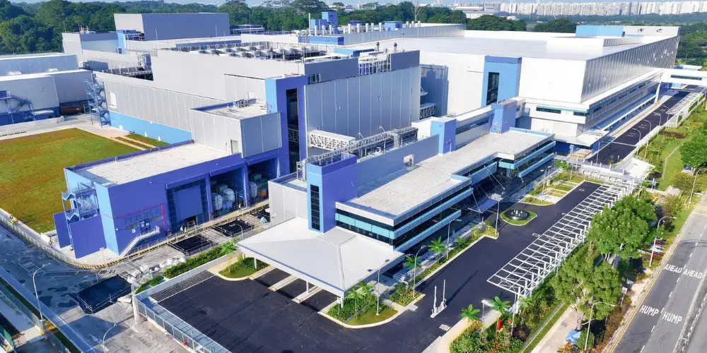
Dholera SIR (Special Investment Region) was not a random pick. A chip fab needs three things in abundance: ultra-clean power, enormous volumes of pure water, and land that will not vibrate. Dholera SIR was planned from a blank slate with wide roads, dedicated utility corridors, a solar power park nearby and an international airport under development.
The Gujarat government also declared a Special Economic Zone for the site, adding tax and customs benefits on top of central incentives from the India Semiconductor Mission. Very few places in India could have offered this package. Dholera could — which is exactly why the TATA semiconductor plant landed here.
What Kind of Chips Will the Dholera Fab Make?
The fab is designed to produce analog and logic integrated circuits on 28nm to 110nm technology nodes, with a planned capacity of 50,000 wafers per month at full scale.
These are not the bleeding-edge chips inside a flagship AI server — and that is deliberate. This node range covers the workhorse chips the world actually consumes in bulk:
- Power management ICs
- Display driver chips
- Microcontrollers (MCUs) for cars and appliances
- High-performance computing logic
- Chips for automotive, IoT, wireless and data storage
Electric vehicles alone use hundreds of such chips. Mature nodes are also where demand is steadiest and margins are most predictable — a sensible place for a first-time fab to start.
Over 20,000 Jobs and a Whole New Ecosystem

The Tata Semiconductor Dholera plant is expected to create more than 20,000 direct and indirect skilled jobs. But the headline number understates the real effect.
A fab pulls an entire ecosystem behind it: chemical and gas suppliers, ultra-pure water plants, precision equipment servicing, cleanroom maintenance, logistics, testing labs and design houses. Tata Electronics has already tied up with premier institutes to train engineers and technicians, and signed a strategic partnership with Dutch lithography giant ASML to strengthen the equipment side. For young engineers in Gujarat and across India, a career path that once required moving to Taiwan, Korea or the US is opening up at home.
What It Means for Make in India and Self-Reliance
India imports the overwhelming majority of the chips it uses. Every global supply shock — a pandemic, a shipping delay, a geopolitical flare-up — hits Indian carmakers and electronics brands directly.
Domestic fabrication does not fix that overnight, but it changes the starting position. A working fab in Dholera gives India a seat at the table in the global semiconductor supply chain and real leverage in strategic sectors like defence, telecom and medical electronics. This is what “Aatmanirbhar Bharat” looks like in practice — slow, capital-heavy, and genuinely structural.
Where the Project Stands Right Now
Construction has crossed the halfway mark. Foundations are complete, and the two phases that actually determine whether a fab works — cleanroom installation and equipment calibration — are underway. Advanced lithography tools have been secured from ASML.
Trial production is targeted for around the end of 2026, with commercial operations to follow. Timelines on projects of this complexity do shift, and some industry reports suggest the fab may begin at a more conservative node than originally announced. That is normal for a first fab anywhere in the world — Taiwan, Korea and the US all took years to get their first plants stable.
Dholera: From Empty Plains to Global Tech Hub
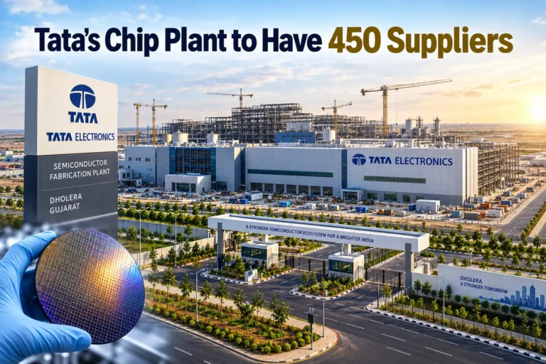
The chip plant is the anchor, not the whole story. Dholera SIR is being developed as a planned smart city with an expressway to Ahmedabad, a metro-rail link, a greenfield international airport and a massive renewable energy park. Land values and investor interest in the region have moved sharply since the project was announced.
If the fab succeeds, Dholera stops being “the place where the Tata plant is” and becomes India’s semiconductor address — the way Hsinchu is Taiwan’s.
The Bottom Line
The TATA semiconductor project in Dholera is India’s first serious attempt at making chips, not just designing and assembling them. It will take years to prove out. But the concrete is poured, the cleanrooms are going up, and the equipment is arriving. India’s chip era has genuinely begun — and it begins in Dholera.
Frequently Asked Questions (FAQs)
It is being built in Dholera SIR (Special Investment Region), a planned smart city and industrial zone in Ahmedabad district, Gujarat.
Powerchip Semiconductor Manufacturing Corporation (PSMC), a Taiwanese foundry, is the technology partner providing process technology and manufacturing expertise.
Up to ₹91,000 crore (roughly US$11 billion), making it one of India’s largest single industrial investments.
Analog and logic ICs on 28nm to 110nm nodes — power management chips, display drivers, microcontrollers and computing logic for automotive, IoT, communications and data storage.
Trial production is targeted for around late 2026, with commercial output expected to follow. Timelines may be revised as construction progresses.






2 thoughts on “India Enters the Chip Era: Tata & Taiwan’s PSMC Build India’s First Semiconductor Plant in Dholera”