

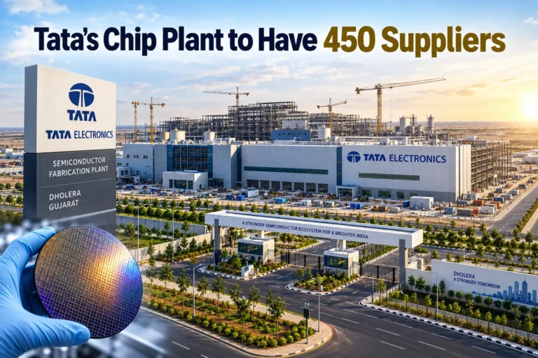
India’s semiconductor ambitions just took a decisive leap forward. The Tata Semiconductor Dholera fab, the country’s first commercial chip fabrication plant, has cleared two major milestones in quick succession — official Special Economic Zone (SEZ) notification and a strategic lithography partnership with Dutch equipment giant ASML. Together, these developments push Tata’s ₹91,000 crore Gujarat project from paperwork and groundwork into a genuinely industrial phase.
1. SEZ Officially Notified for Tata’s Dholera Fab
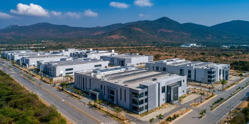
The Ministry of Commerce and Industry has formally notified an SEZ for Tata Semiconductor Manufacturing Private Limited at Dholera, Gujarat. The zone spans 66.166 hectares within Dholera’s industrial area under Town Planning Scheme 2A, and it is expected to generate close to 21,000 jobs once fully operational. This makes it India’s first chip fabrication plant to receive such SEZ status — a significant regulatory and symbolic milestone for the country’s electronics manufacturing push.
2. The Policy Reforms That Made It Possible
The notification didn’t happen in isolation. It follows amendments to the SEZ Rules, 2006, introduced in June 2025, specifically designed to accommodate the unique demands of semiconductor manufacturing. Among the key changes: the minimum land requirement for semiconductor and electronics component SEZs was slashed from 50 hectares to just 10 hectares, encumbrance norms were made more flexible, free-of-cost supplies were folded into Net Foreign Exchange calculations, and companies were permitted to sell into the Domestic Tariff Area on payment of applicable duties. These reforms were tailor-made to unblock exactly the kind of large, capital-intensive project Tata is building. The SEZ itself will support electronic hardware, software, and IT-enabled services, backed by a dedicated approval committee drawing from the commerce ministry, tax authorities, customs, and the Gujarat state government.
3. Why the Dholera Fab Is a Big Deal for India
The Dholera fab isn’t just another factory announcement. It represents India’s first attempt at front-end chip fabrication — the complex, precision-driven process of actually manufacturing semiconductor wafers, as opposed to backend work like assembly, testing, and packaging, which India has handled for years. The plant is a joint venture between Tata Electronics and Taiwan’s Powerchip Semiconductor Manufacturing Corporation (PSMC), approved by the Union Cabinet in February 2024, and sits within the well-connected Delhi-Mumbai Industrial Corridor.
4. Production Scale and Chip Focus
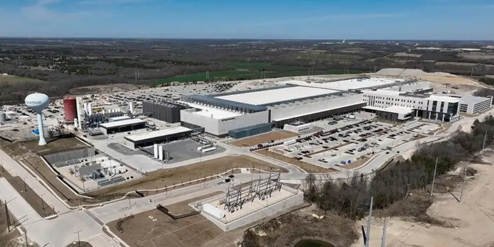
At full capacity, the facility is designed to produce 50,000 wafer starts per month, with each wafer yielding thousands of individual chips — translating to billions of chips annually once operations mature. The plant will focus on process technology nodes ranging from 28nm to 110nm, covering power management ICs, display drivers, microcontrollers, and other chips used heavily in automotive, mobile, industrial, and AI-adjacent applications. These aren’t cutting-edge chips for flagship smartphones, but the workhorse semiconductors that power everyday electronics — a segment where global supply chains have repeatedly shown fragility.
5. ASML Partnership Brings Critical Lithography Technology
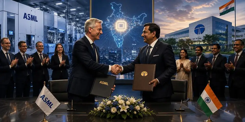
If the SEZ notification addressed the regulatory side, the ASML deal tackles the technology side. Tata Electronics and ASML have signed a Memorandum of Understanding under which ASML will supply its lithography tools and technical expertise to support the Dholera fab’s setup and ramp-up. This matters enormously: ASML holds a near-monopoly on advanced lithography equipment — the machines that etch circuit patterns onto silicon wafers, arguably the single most critical and technically demanding step in chip manufacturing. Without reliable access to this equipment, no fab, however well-funded, can realistically hit its production targets.
6. How the Deal Came Together
The partnership was announced during Prime Minister Narendra Modi’s visit to the Netherlands, with Tata Electronics CEO Randhir Thakur and ASML CEO Christophe Fouquet signing the agreement in the presence of both Modi and Dutch Prime Minister Rob Jetten. Beyond equipment supply, the collaboration extends to training local talent, building lithography-specific skills, strengthening supply chain resilience, and jointly developing R&D infrastructure. Thakur called it key to ensuring the “timely ramp” of the fab, while Fouquet pointed to India’s semiconductor sector as offering “compelling opportunities” for ASML’s own long-term regional ambitions.
7. What Comes Next for India’s Chip Mission
With regulatory clearance secured and a critical technology partner locked in, the Dholera fab is now squarely in execution mode, targeted to commence operations by 2027. Combined with earlier moves — including the PSMC technology tie-up and a separate agreement with Merck for chemicals and materials support — Tata is steadily assembling the full ecosystem a chip fab needs: land, regulatory clearance, process technology, equipment, and specialty materials. For India, the stakes go well beyond one company’s balance sheet. A working domestic fab reduces reliance on imported chips, strengthens supply chain security, and positions Gujarat — alongside emerging hubs like Assam and Karnataka — as a genuine node in the global semiconductor map. If Tata can keep this momentum through construction and equipment installation, Dholera could become the proof point India’s semiconductor mission needed.
FAQs
It’s India’s first commercial chip fabrication plant, a ₹91,000 crore joint venture between Tata Electronics and Taiwan’s PSMC, being built in Dholera, Gujarat.
The government has officially designated 66.166 hectares of the Dholera site as a Special Economic Zone, unlocking tax benefits and streamlined approvals, and paving the way for around 21,000 jobs.
ASML, the world leader in lithography equipment, will supply its lithography tools and expertise to help set up and ramp up the Dholera fab.
The plant is targeted to begin operations by 2027, with construction currently underway.
It will manufacture chips using 28nm to 110nm process nodes, mainly for automotive, mobile, industrial, and AI-related applications, at a planned capacity of 50,000 wafers per month.






3 thoughts on “Tata Semiconductor Project Sees Major Progress: SEZ Notified, ASML Partnership Signed”