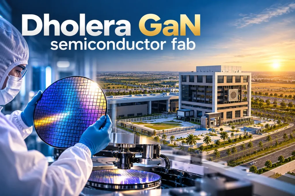
India’s chip ambitions just gained a brighter edge, quite literally. The Union Cabinet has approved Crystal Matrix’s proposal to set up the country’s first compound semiconductor facility built around Gallium Nitride (GaN) in Dholera Special Investment Region (SIR), Gujarat.
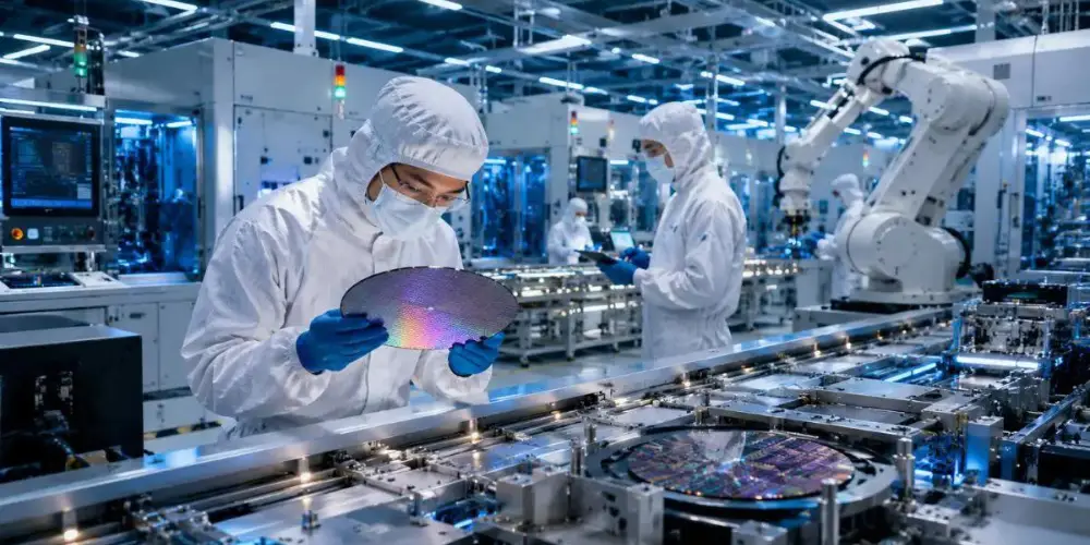
This Dholera GaN semiconductor fab will combine wafer fabrication with ATMP (Assembly, Testing, Marking and Packaging) under one roof. Its focus is clear: power the next generation of Mini-LED and Micro-LED displays.
Here is a closer look at what the project involves, why GaN matters, and what it means for Gujarat and the wider Indian economy.
1. The Project at a Glance
Crystal Matrix’s proposal was cleared under the Compound Semiconductor Scheme of the India Semiconductor Mission (ISM). The key numbers tell the story:
| Parameter | Details |
| Investment | ₹3,068 crore |
| Location | Dholera SIR, Gujarat |
| Land allotted | 40 acres |
| Wafer output | 24,000 sets of RGB GaN wafers per year |
| Display output | 72,000 sq. m of Mini/Micro-LED panels per year |
| Employment | 1,600+ direct jobs |
It is a mid-sized investment by global fab standards. But it opens an entirely new category for Indian manufacturing.
2. Why Gallium Nitride Is a Big Deal
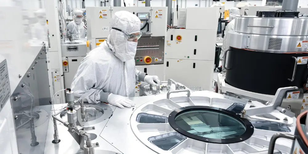
Most chips we hear about are made from silicon. Compound semiconductors are different. They combine two or more elements, such as gallium and nitrogen, to achieve properties silicon cannot easily match.
GaN stands out for three reasons:
- Efficient light emission: It is the backbone material for blue and green LEDs, and therefore for full-colour LED displays.
- High power handling: It works well in fast chargers, EV power systems and data centre power supplies.
- Heat tolerance: GaN devices operate reliably at higher temperatures and voltages.
For the Dholera unit, the display angle is the priority. Producing RGB GaN epitaxy wafers means India can build the light-emitting layers that sit at the heart of modern screens.
3. Mini-LED and Micro-LED: The Screens of Tomorrow
If you have seen a premium TV or laptop recently, you may have noticed “Mini-LED” on the spec sheet. Micro-LED goes a step further.
Mini-LED uses thousands of tiny LEDs as a backlight. This allows sharper contrast and deeper blacks than conventional LCD screens.
Micro-LED removes the backlight entirely. Each pixel emits its own light, delivering high brightness, long life and excellent colour accuracy.
These technologies are expanding into televisions, smartwatches, AR/VR headsets, automotive dashboards and large digital signage. Today, India imports nearly all of these components. A domestic supply of GaN wafers and finished panels changes that equation.
4. Why Dholera Keeps Winning Semiconductor Projects
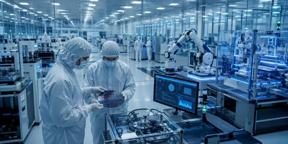
Dholera SIR is fast becoming India’s chip corridor. The region already hosts major semiconductor investments, and this approval adds a new layer: compound semiconductors.
Several factors make Dholera attractive:
- Planned infrastructure: Wide roads, dedicated utility corridors and large land parcels designed for heavy industry.
- Reliable power and water: Both are critical for wafer fabrication.
- Policy support: Gujarat’s state incentives work alongside central ISM benefits.
- Connectivity: Proximity to Ahmedabad, upcoming expressways and the Dholera airport project.
Clustering matters in semiconductors. Suppliers, gas providers, equipment service firms and skilled workers tend to gather where multiple fabs operate. Each new project strengthens that ecosystem.
5. Jobs, Skills and the Local Economy
The project is expected to create more than 1,600 direct jobs. These will include process engineers, cleanroom technicians, quality specialists and maintenance staff.
The indirect effect could be even larger. Construction, logistics, housing, hospitality and component suppliers will all see new demand around the site.
Equally important is skill-building. Compound semiconductor manufacturing requires specialised know-how that India has lacked. Training a workforce in epitaxy, LED fabrication and advanced packaging creates talent that can serve future projects too.
6. What This Means for Aatmanirbhar Bharat
India’s display and electronics market is growing rapidly, yet its component base remains import-heavy. A GaN fab with integrated ATMP helps in several ways:
- Reduces import dependence for high-value display components.
- Improves supply chain resilience against global disruptions.
- Supports electronics makers under PLI schemes with local inputs.
- Positions India as a potential exporter of advanced display components.
It also signals that ISM is moving beyond silicon logic and memory chips. Compound semiconductors are a strategic niche, and early entry gives India a stronger foothold.
7. The Road Ahead
Approval is only the first step. Building a fab involves cleanroom construction, equipment installation, process qualification and customer validation. Timelines in this industry are often measured in years.
Still, the direction is promising. With ISM backing, a dedicated site and a clear product focus, the Dholera GaN project could become a model for future compound semiconductor investments in India.
For investors, industry watchers and job seekers, Dholera is a name worth following closely.
Frequently Asked Questions
Crystal Matrix is setting up the facility after receiving Union Cabinet approval.
The total investment is ₹3,068 crore.
It will produce RGB GaN epitaxy wafers and Mini/Micro-LED display panels.
24,000 sets of RGB GaN wafers and 72,000 sq. m of Mini/Micro-LED panels each year.
The project has been allotted 40 acres in Dholera SIR.